A one side double-coated solid bleached cartonboard SBB Algro Design has a remarkable silky touch thats perfect for lamination to solid and corrugated boards. Allegro Package Designer - Cadence Design Systems Introduction to Allegro PCB Designer PCB Stack-up and Visibility Window.
Ic Packagers An Introduction To Allegro Package Designer Plus In 17 4 Ic Packaging And Sip Cadence Blogs Cadence Community
It supports all packaging methods including PGA BGA micro-BGA chip scale as well as flip-chip and wirebond attach methods.

. Full online design-rule checking supports the complex unique requirements of. Click on File - New. Allegro PCB Design Tutorial This tutorial is intended for beginners in printed circuit board design who wish to complete a board using Cadence Allegro Tool.
Part 7 In this tutorial I will discuss about the Visibility window and PCB layers in my previous tutorials I have discussed about the Options and Find windows so Visibility window is another window besides these two windows and also used frequently. In the Drawing Type Select Package Symbol. It provides academic executives consultants instructors IT specialists librarians LIS students.
Cadence is using the Squeak open-source Smalltalk platform for research and development work. Download Allegro Package Designer Tutorial PDF Ebook online PDF Read Online Allegro Package Designer Tutorial mobipocket B. Click on Start - Allegro SBP 152 - PCB Editor - Select Allegro PCB Design 610 PCB Design Expert - Click OKThis will open up the Allegro software.
Allegro Package Designer 610 includes all the functionality and features you need to design todays advanced packages. Allegro 5 can be found in the allegro package on homebrewSee the wiki tutorial for more details. Cadence provides the only platform built to allow you to design and optimize the entire system from chip package and board for true multi-fabric design.
Allegro Use Hilight Dehilight Tool Tutorial 5. Get Free Allegro Package Designer Tutorial Allegro Package Designer Tutorial 6bc3772449407956b1f77420df632b41 Best PCB Design Software in 2022. You develop a process flow create cross section and design constraints construct.
For this tutorial we will be creating the symbols for the 0603 resistor and the two pin Header. Benefits no washboarding effect. Constraint Manager Tutorial Back-End This book contains step-by-step exercises to familiarize you with using Constraint Manager with Allegro PCB 200 and 600 Series and Allegro SI SigXplorer 200 or 600 Series.
Introcution to Copper Shapes in Allegro. Compare Reviews on. Read Online Allegro Package Designer Tutorial This book is written to promote academic strategic management and envision future innovations for academic library resources services and instructions in the digital age.
About Press Copyright Contact us Creators Advertise Developers Terms Privacy Policy Safety How YouTube works Test new features Press Copyright Contact us Creators. A robust set of packaging-specific features are available such as on-the-fly library development connectivity generationoptimization multi-tiered wire. Allegro Package Designer is the industry-standard solution for traditional IC package design.
For Linux distributions based on Ubuntu and Ubuntu itself you can download binary packages for Allegro 5 by adding the a PPA to your software sources and then installing the relevant packages. Fresh and clean look highest resistance to aging. Cadence Allegro Package Designer Plus enables constraint-driven correct-by-design package substrate layout.
Complete your design fast and confidently with 64-bit performance an enhanced GPU engine for acceleration and quality rendering dynamic updates for interactive routing and shapes comprehensive rules and more. Allegro Use Show Measure Grid Tutorial 6. You can access a Flash-based multimedia demo of this tutorial in the books appendix.
Allegro Use Slide Tool Tutorial 4. Cadence Allegro PCB Design Platform. Brief tutorial of C and games programming in Allegro containing a lot of examples and a game programmed in C Allegro including the source code.
With Allegro products you can place and route a. Introcution to Stackup in Allegro. The Cadence Allegro FREE Physical Viewer is a free download that allows you to view and plot databases from Allegro PCB Editor Allegro Package Designer and Allegro PCB SI technology.
With direct connections to Virtuoso. Allegro Package Designer Tutorial Physical layout systems of printed circuit boards PCBs created with Allegro Microelectronic packages such as multichip modules MCMs or single chip modules SCMs created with Advanced Package Designer APD. See the wiki tutorial for more details.
It supports all packaging methods including LGA PGA BGA micro-BGA and chip scale using both flip-chip and wirebond die attach methods. Online Library Allegro Package Designer Tutorial Allegro Package Designer Plus DS Substrate design consists of layout of all signals from the package balls to the wirebond pads in case of Wire Bond or to the bump pads in case of Flip-Chip. Download your FREE Physical Viewer today.
The Ultimate PCB Design Experience. This site will show all you need to know in order to create your own video games coded in C. 4 days In this course you use the Allegro Package Designer system for the design and specification of manufacturing single-chip modules for single- double- or multilayered analog and digital packages.
With Allegro Design Entry HDL. Its proven design environment focuses on single staticfixed chip packages. Introcution to Nets in Allegro.
This tutorial is for Windows XP but most of the things should be easy to be extended for Linux or Unix. For chip implementation and tight integration with Allegro for package and PCB analysis design teams are finally able to design with the entire system in. It supports a full front-to-back physical implementation flow for single- and multi-die BGALGA package design.
Read More Free Read vhlcentral answer key leccion 4 prueba Free Download PDF. INTRODUCTION Those who had experience with one or more PCB design tool may skip this page. Whether the BGA substrate design is done by the assembly house or by an external company specializing in.
Hi I can see that none have answered this but in the directory CCadenceSPB_157docwb_tut there are tutorials with files for Allegro Package Design. Introduction to Allegro PCB Designer. In the drawing name write R0603_1.
Allegro Use Add Connect Tool Tutorial 3. Cartonboard bulk and stiffness versus other liners.

Tutorial Orcad Allegro Finding Nets And Components Youtube

Allegro Downloads

Cadence Allegro Advanced Package Designer Plus Ema Design Automation

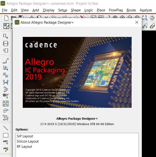
Allegro Package Designer Plus

Allegro Package Designer Plus Sip Layout Option

Sigrity Tech Tip How Ic Package Designers Can Find And Fix Electrical Problems Youtube

Cadence Allegro Advanced Package Designer Plus Ema Design Automation
Allegro Package Designer Youtube
0 comments
Post a Comment